Table Of Content
Other design software platforms claim to integrate features, but they still separate critical design tools into addons without providing the guidance new users need to be successful. Instead, you should use design software that gathers all your design tools in one place alongside design resources. Once your board has passed the final DRC, you need to generate the design files for your manufacturer.
PCB design is like designing a city
A. Multi-layer PCBs offer several advantages, including higher component density, improved signal integrity, enhanced thermal management, and increased design flexibility. They enable the creation of more complex and compact electronic devices. Flexible PCBs, constructed from thin, flexible materials like polyimide or polyester, can bend and twist without damaging the conductive traces. This flexibility makes them ideal for applications requiring conformity to irregular shapes or resistance to vibration, such as wearable electronics, medical devices, and aerospace systems. The ability to bend and fold flexible PCBs allows for more compact and space-efficient designs in these applications. When designing thermal vias, it is important to consider factors such as via size, spacing, and placement.
Book Excerpt: 'The Printed Circuit Designer's Guide to... Manufacturing Driven Design' - I-Connect007
Book Excerpt: 'The Printed Circuit Designer's Guide to... Manufacturing Driven Design'.
Posted: Thu, 03 Aug 2023 07:00:00 GMT [source]
Traffic Light PCB Layout: Tips and Tricks for Efficient Design
Electromagnetic radiation can cause crosstalk when high-frequency signals radiate energy that is picked up by nearby traces or components. Crosstalk is a phenomenon that occurs when a signal from one trace or component unintentionally couples with another, causing interference and degrading signal quality. This can lead to signal distortion, false triggering, and other issues that can compromise the performance and reliability of the electronic device.
Step 2: Create a Blank PCB Layout
In conclusion, proper testing and troubleshooting are essential when working with traffic light PCB layouts to ensure that they function correctly and reliably. By following the steps outlined above, you can identify and resolve any issues with the PCB, ensuring that it is ready for installation. The components on the PCB must be arranged in a specific way to ensure that they function correctly. The layout must be designed to minimize the risk of interference between components, and to ensure that the board is easy to manufacture and assemble.
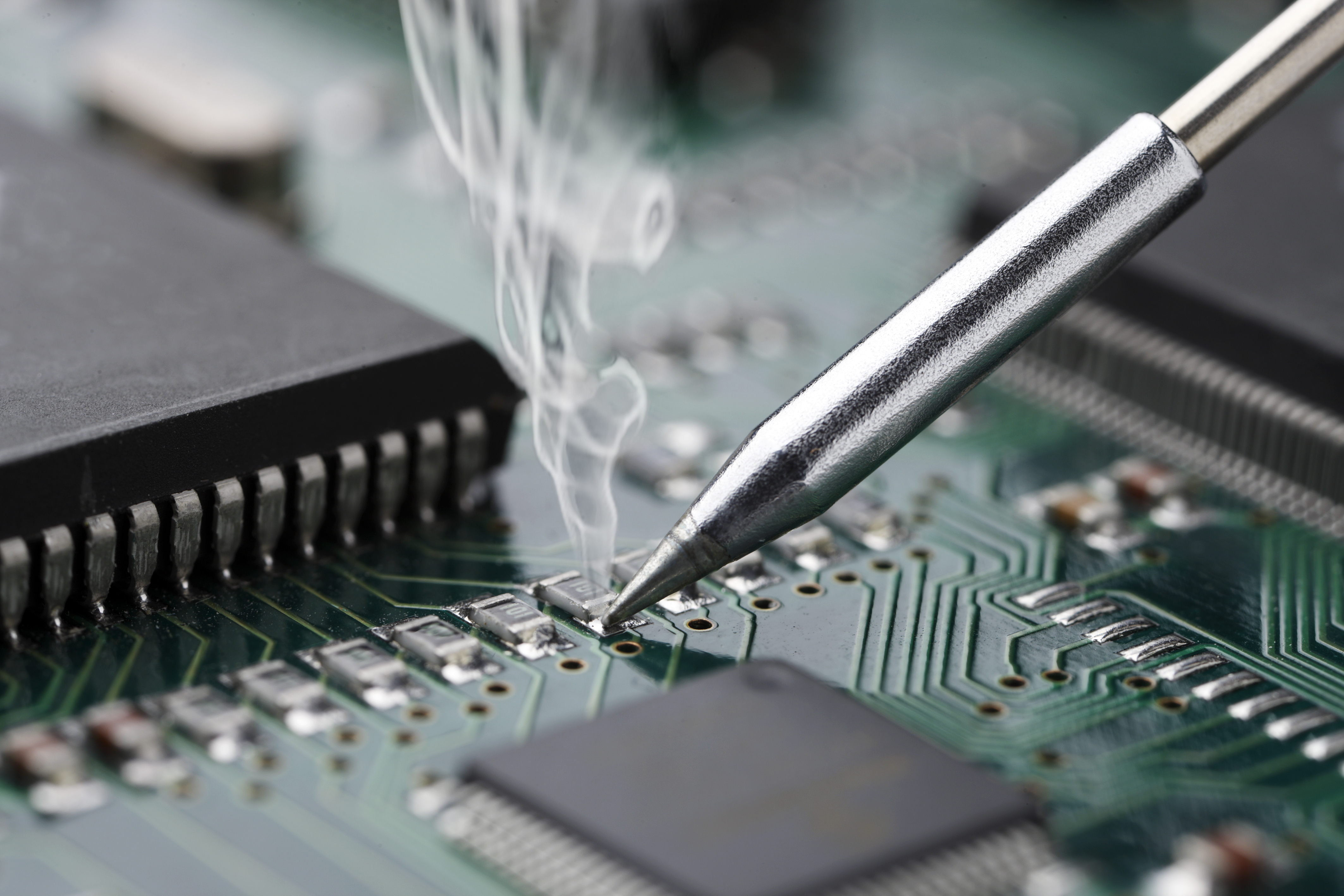
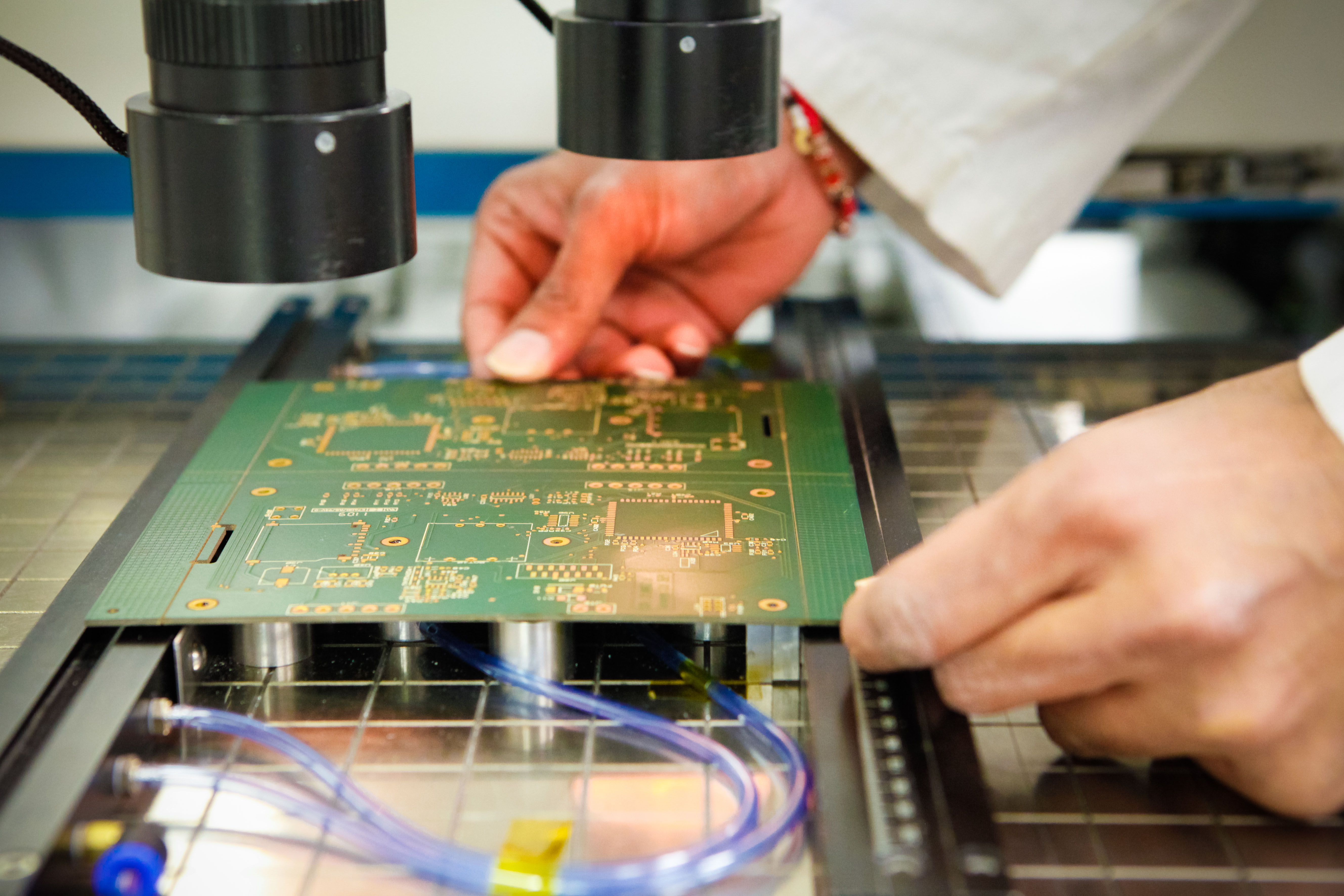
Designers must carefully consider various factors to create PCBs that meet the specific requirements of their applications. From design to final artwork, the journey of a printed circuit board is fascinating. Every step in the process requires precision and attention to detail to ensure a reliable and functional end product. PCB assembly involves soldering the electronic components onto the board. That can be done manually or with the help of automated machinery, depending on the complexity and volume of the production. The components are carefully placed and soldered onto the board, following the design specifications.
Schematic Design
PCB designers follow a general PCB design process methodology, and there are some important things to consider in your schematic and layout before you get started. Thinking about the answers to these questions can help you avoid common problems in PCB design process methodology and determine the right PCB design process methodology for your next idea. With the circuit board layout verified you are ready to add labels, identifiers, markings, logos, or any other imagery to your board.
Use PCB Tools for High-Quality Design
He currently provides research, design, and marketing services to companies in the electronics industry. Prior to working in the PCB industry, he taught at Portland State University and conducted research on random laser theory, materials, and stability. His background in scientific research spans topics in nanoparticle lasers, electronic and optoelectronic semiconductor devices, environmental sensors, and stochastics.
Create Your PCB Design Process Methodology in Altium Designer
The width of the traces and the spacing between them are critical for maintaining the required impedance and preventing signal degradation. Consult the design guidelines provided by your PCB manufacturer to determine the appropriate trace widths and spacing for your design. While they are necessary, excessive use of vias can increase the complexity of the design and affect signal integrity.
If you’ve ever used a new piece of software, you know about the learning curve involved. With so many different PCB design packages on the market, getting up to speed quickly requires design software that places all of your critical design tools in a single interface. Why not purchase PCB design software that shows you how to be successful?
In a high-speed digital design, designers may focus on proper trace spacing and termination to minimize reflections and maintain signal integrity. To minimize these issues, designers must ensure that the impedance of the signal path is matched to the impedance of the source and load. This is typically achieved through the use of controlled impedance traces, which are designed to have a specific characteristic impedance based on factors such as trace width, thickness, and spacing. Design Rule Checking (DRC) is a process that verifies the PCB layout against a set of predefined design rules, such as minimum trace widths, clearances, and via sizes. [3] These rules are established by the PCB fabrication house to ensure that the design can be manufactured without issues. DRC checks help identify potential manufacturing problems, such as shorts, opens, and clearance violations, before the design is sent for fabrication.
A PCB is sort of like a layer cake or lasagna- there are alternating layers of different materials which are laminated together with heat and adhesive such that the result is a single object. Have your computer with the PCB Design close by so that you can check the orientation and value of components if needed. If that’s not possible, print out the schematic with values and the board layout. Surface mount components are smaller, so they take up much less space. That said, it just takes a bit of practice to get used to surface mount components. At the assembly facility, the board is loaded with the components it needs and runs through different soldering processes, depending on the type of components being used.
You need to know which pieces go where and how everything fits together, as well as how many layers your board will be and the materials to use. When designing a PCB board layout, you need to be as prepared as possible. Firstly, you’ll need to know what it’s used for before going too much further; take a look through our previous blog post if you’re unsure. The industry's best ECAD software should be easy to use and easy to learn, and it should include a complete set of design features.


No comments:
Post a Comment